
Dirac semimetals
Graphene and topological insulators are two materials that are generating tremendous interest in the new materials market. Now Dirac semimetals have joined the forefront. All these materials have interesting physical properties, their electron structure is unique, and they provide room for many new discoveries.
Nodal Dirac semimetals are materials that, from an electronic structure point of view, can be understood as a three-dimensional analog of graphene. In graphene, as in semimetals, one can find Dirac points. Discrete Dirac points are formed at the crossings of the conduction and valence bands. Examples of such a compound are Na3Bi and Cd3As2.
Interesting electron structure of LaAgSb2
Reading previous publications on the compound LaAgSb2, which is a Dirac semimetal, SOLARIS scientists became interested in its nontrivial topological character. In cooperation with specialists from the Institute of Nuclear Physics in Krakow, they made theoretical calculations, which they then decided to confirm experimentally. For the study, the authors used the angle-resolved photoelectron spectroscopy (ARPES) technique available on the URANOS beamline. The results obtained are surprising and contradict previous predictions about this compound.
Marcin Rosmus, the first author of the paper, says more about the publication:
"Our experiment supported by theoretical calculations has shown the existence of Dirac nodal lines that result from the symmetry of the system or the disappearance of spin-orbit splitting. Moreover, we showed that the linear bands do not form Dirac surface states, which was confirmed by theoretical calculations performed for different sample surface terminations. Previous predictions for this compound spoke of the existence of a Dirac-like structure near the Fermi level. Our results contradict this."
Fig.1. The electronic band structure along a series of paths presented on the Fermi surface (a). Theoretical spectral function (left) and band structure (right) along the Γ–M path for a finite system (b) and related bulk band structure (c). Panels (d) present band structures calculated for the slab geometry. Theoretical prediction of the spectral function within the surface Green’s function calculation is presented in (e). Panels (f–k) show the experimental spectra recorded with the ARPES measurements with hν=66 eV at a temperature of 12 K (left panels) and their 2D curvatures (right panels) along different cuts from (a).
Link to the publication:
Written by: Marcin Rosmus
Weyl semimetal
Niobium phosphide is an interesting material, representative of the Weyl semimetal family. Weyl semimetals are characterized by the presence of Weyl fermions (which are massless particles with spin 1/2) and Fermi arcs on the surface. Ultra-high mobility of charged Weyl fermions in semimetals may find its applications in electronics and computer science. Research on topological semimetals provides not only physical curiosities but also leads to new electronic materials.
The researchers from the Institute of Physics in Warsaw have grown the single crystals of NbP and characterized their surface properties by using angle-resolved photoemission spectroscopy (ARPES) at URANOS (previous UARPES) beamline at SOLARIS.
Unexpected FS modification
Ashutosh S. Wadge (International Research Centre MagTop, Institute of Physics PAS), the first author of the paper published in Phys. Rev. B , explains the phenomenon in detail as follows:
Niobium monophosphide NbP is a representative example of so-called Weyl semimetals (WSM). These materials have an unusual band structure in which the linearly dispersed valence and conduction bands meet at discrete Weyl points (WP). The other important feature of WSM is surface Fermi arcs (SFAs) that originate from and terminate at the surface projection of a pair of Weyl points of opposite chirality. SFAs are unique open Fermi surfaces (FS) that are unlike closed FS in conventional materials and give rise to many exotic phenomena, such as anomalous quantum oscillations, chiral magnetic effects, 3-dimensional quantum Hall effect, and anomalous electromagnetic wave transmission. Since these intriguing phenomena mainly involve SFAs, hence, from the point of view of basic research and applications, it is very relevant to find an effective way of controlling and modification of SFAs, e.g., of switching them between pairs of Weyl points. We studied surface electronic properties of the P-terminated and Nb-terminated surfaces of NbP with Pb or Nb deposition. An unexpected FS modification has been observed: one monolayer (ML) of Pb influenced the Fermi arcs in such a way that they exchanged the pair of Weyl points and connected the two adjacent Brillouin zones. This change in the Fermi surface is attributed to a topological Lifshitz transition (TLT) with preserved topological characteristics even after surface perturbation. Interestingly, 1.9 ML of Pb on Nb-terminated NbP showed an ordinary Lifshitz transition with no effect on Fermi arcs, 0.8 ML of Nb modified P-terminated Fermi surface with partial TLT.
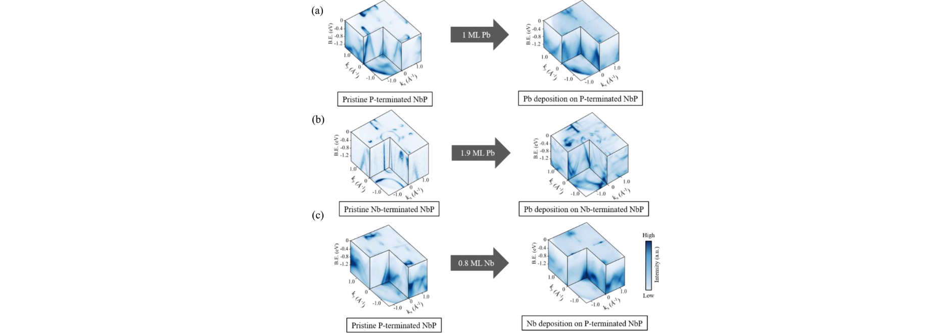
Fig. 1. The comparisons between 3D intensity plots of (a) pristine P-terminated NbP as well as 1 ML of Pb deposited on P-terminated NbP, (b) pristine Nb-terminated NbP and modifications obtained after 1.9 ML Pb deposition, and (c) pristine P-terminated NbP and modification obtained after 0.8 ML Nb deposited on P-terminated NbP with explaining the modification of band structure. Figure reprinted with permission from A.S. Wadge et.al, Physical Review B 105, 235304 (2022). Copyright (2022) by American Physical Society.
Link to the publication:
Magnetic Topological Insulators
Joanna Sitnicka, the PhD student at the Faculty of Physics, University of Warsaw, and the first author of the publication is summarizing the main findings in the publication for us:
We studied the family of intrinsic magnetic topological insulators MnBi2Te4/(Bi2Te3)n. The materials structure is an alternating sequence of magnetic MnBi2Te4 seven-layers (SLs) and Bi2Te3 five-layers (QLs) (Fig. 1(a)). We performed structural and chemical composition analysis of ferromagnetic samples of MnBi2Te4/(Bi2Te3)n, with a few different distances n between adjacent SLs and correlated them with magnetic properties studied by ferromagnetic resonance spectroscopy (FMR) and with properties of electronic surface band structure investigated by angle-resolved photoemission spectroscopy (ARPES). Our structural analysis revealed disorder effects in a form of Mn substituting Bi in QLs and Mn missing in SLs (Fig. 1(b)). Such migration of Mn between SLs and otherwise non-magnetic QLs, which is schematically shown in Fig. 1(c), has systemic consequences for the material. It induces ferromagnetic coupling of Mn-depleted SLs with Mn-doped QLs, which is seen in FMR as an acoustic and optical resonance mode of the two coupled spin subsystems (Fig. 1(d)). It also strongly influences the surface band structure. ARPES measurements compared with density functional theory studies show that Mn disorder within an SL leads to delocalization of electron wave functions and strongly changes the structure of surface bands as compared to the ideal MnBi2Te4/(Bi2Te3)n (Fig. 1(e)).
Fig. 1 (a) High-angle annular dark field (HAADF) scanning transmission electron microscopy image of a SL in QL matrix. Bi as the heaviest element gives the highest intensity to the image. Manganese is incorporated in the middle layer of the SL. SL and neighboring QL are separated by the van der Waals gap. (b) Fragment of the MnBi2Te4/(Bi2Te3)n superlattice in one of the studied samples. Energy dispersive x-ray analysis mapping with the distribution of Mn atoms shown in yellow and Bi atoms shown in blue respectively shows substitution of Mn on Bi site in Bi2Te3. (c) A schematic representation of disorder in the distribution of Mn – an absence of Mn in SLs and its presence in QLs. (d) (upper panel) FMR in one of tested samples shows a separation of acoustic and optical resonance mode of coupled SLs and QLs. The lower panel shows anisotropy of the resonance signals at 5 K. Remarkably, the two modes never cross in the angular dependence, which is characteristic for FMR in coupled films and allows to distinguish them from the uncoupled layers. (e) ARPES data of the disordered MnBi2Te4/(Bi2Te3)n obtained along Γ→Μ direction at photon energies 54 eV and 20 eV compared with DFT calculations for 2QL-SL-2QL-SL structure with 50% of Mn atoms in SLs replaced by Bi.
Link to the publication:
Antiferromagnetic layered compound Co1/3NbS2
Scientists have used angle-resolved photoemission spectroscopy (at UARPES beamline, SOLARIS Centre) to obtain detailed insights into complex electron-electron and electron–lattice interactions in the solid. The observed electronic structure of Co1/3NbS2 resembles the parent material 2H-NbS2, however, some significant departures are observed, which cannot be explained by the rigid band shift with minor deformation of bands.
The first author of the publication, Dr. Petar Popčević, explains the main idea behind the conducted experiment:
The materials made of alternating metallic and magnetic atomic layers continue to promise and deliver new magnetic orderings and electronic states. Co1/3NbS2 represents such material, with pronounced magnetic frustration and the lowest magnetic ordering temperature among similar systems. The paper brings the study of the electronic structure through angle-resolved photoelectron spectroscopy (ARPES), accompanied by extensive comparison to ab initio calculations and modeling. The data suggest that magnetic Co ions provide the dominant bridges for electronic conduction in the direction perpendicular to layers. The nature of the connection strongly depends on magnetic configuration. The strong mixing between itinerant and magnetic degrees of freedom is argued to be responsible for the band observed at the Fermi level, in the form of a necklace composed of shallow and wide electronic pockets. The band is entirely unforeseen by usual electronic structure calculations, indicating an example of a strongly correlated electronic system where the coupling between layers plays an exquisite role.
Fig. 1.I. (a) The electronic spectra calculated for Co1/3NbS2 in the particular antiferromagnetically ordered state. The electronic bands are shown unfolded along M0ΓK0 line of the Brillouin zone of 2H-NbS2, averaged over three equivalent directions by hexagonal symmetry. II. (a) The unfolded spectra of the system were modeled through the tight-binding reparameterization, with the parameters initially taken from our DFT/Wannier calculation. Very few modifications are inspired by studies of the effects of strong electron correlations in other systems. I & II (b) The comparison between the measured and calculated spectra along the Γ − K0 line. I & II(c) The comparison between the calculated and experimental spectra at the Fermi level. The dotted lines mark the boundary of the first Brillouin zone of Co1/3NbS2.
Link to the publication: